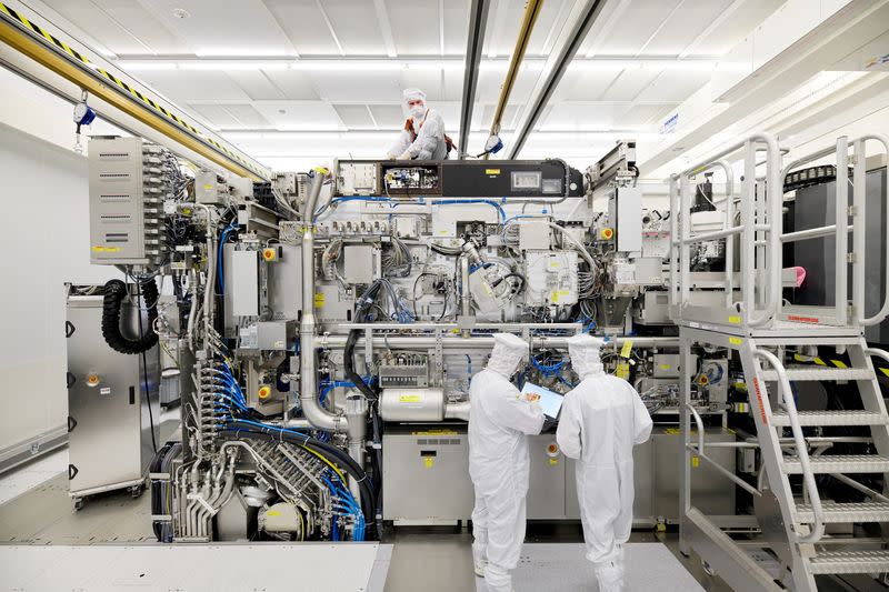
In a high-security laboratory in Shenzhen in southerly China, researchers are improving work with a model chipmaking device that intends to create the innovative chips utilized to power expert system, smart devices and the tools that are crucial to Western armed forces supremacy.
Washington has actually invested years attempting to avoid Beijing obtaining accessibility to this modern technology, however China has actually invested billions of bucks to reproduce a contemporary lithography device.
Reuters has actually discovered that early this year China accomplished a first component of this objective by finishing a huge device that fills up almost a whole flooring and is currently being evaluated. It was developed by a group of previous designers from Dutch semiconductor titan ASML that reverse-engineered the business’s severe ultraviolet lithography devices or EUVs, according to 2 individuals with expertise of the job.
LIKEWISE SEE: Bumper IPO by One More China Chip Company Increases Buzz Worry
EUV devices rest at the heart of a technical Cold Battle. They make use of light beams of severe ultraviolet light to engrave circuits hundreds of times thinner than a human hair onto silicon wafers, presently an ability taken over by the West. The smaller sized the circuits, the a lot more effective the chips.
China’s device is functional and effectively creating severe ultraviolet light, however has actually not yet generated functioning chips, individuals claimed.
In April, ASML chief executive officer Christophe Fouquet claimed that China would certainly require “lots of, several years” to establish such modern technology However the presence of this model, reported by Reuters for the very first time, recommends China might be years more detailed to attaining semiconductor self-reliance than experts prepared for.
Nonetheless, China still deals with significant technological obstacles, especially in reproducing the accuracy optical systems that Western distributors create.
The accessibility of components from older ASML devices on additional markets has actually permitted China to develop a residential model, with the federal government establishing an objective of creating functioning chips on the model by 2028, according to both individuals.
However those near the job state an even more practical target is 2030, which is still years previously than the years that experts thought it would certainly take China to match the West on chips.
Chinese authorities did not reply to ask for remark.

Huawei collaborating a Chinese ‘Manhattan Task’
The advancement notes the conclusion of a six-year federal government campaign to accomplish semiconductor self-sufficiency, among Head of state Xi Jinping’s greatest top priorities. While China’s semiconductor objectives have actually been public, the Shenzhen EUV job has actually been performed in trick, according to individuals.
The job drops under the nation’s semiconductor method, which specify media has actually recognized as being run by Xi Jinping confidant Ding Xuexiang, that heads the Communist Celebration’s Central Scientific research and Innovation Compensation.
Chinese electronic devices gigantic Huawei plays a crucial function collaborating an internet of firms and state research study institutes throughout the nation entailing hundreds of designers, according to both individuals and a 3rd resource.
Individuals defined it as China’s variation of the Manhattan Task, the United States war time initiative to establish the atomic bomb.
” The goal is for China to become able to make sophisticated chips on devices that are completely China-made,” among individuals claimed. “China desires the USA 100% tossed out of its supply chains.”
Huawei, the State Council of China, the Chinese Consular Office in Washington, and China’s Ministry of Sector and Infotech did not reply to ask for remark.
Previously, just one business has actually grasped EUV modern technology: ASML, headquartered in Veldhoven, Netherlands. Its devices, which set you back around $250 million, are crucial for producing one of the most sophisticated chips made by firms like Nvidia and AMD– and generated by chipmakers such as TSMC, Intel, and Samsung.
ASML developed its very first functioning model of EUV modern technology in 2001, and informed Reuters it took almost twenty years and billions of euros in R&D costs prior to it generated its very first readily readily available contribute 2019.
” It makes good sense that firms would certainly intend to reproduce our modern technology, however doing so is no tiny accomplishment,” ASML informed Reuters in a declaration.
ASML’s EUV systems are presently readily available to United States allies, consisting of Taiwan, South Korea, and Japan.
United States export visuals
Beginning in 2018, the USA started pushing the Netherlands to obstruct ASML from marketing EUV systems to China
The limitations broadened in 2022, when the Biden management enforced sweeping export controls made to remove China’s accessibility to sophisticated semiconductor modern technology. No EUV system has actually ever before been offered to a client in China, ASML informed Reuters.
The controls targeted not simply EUV systems however likewise older deep ultraviolet (DUV) lithography devices that create less-advanced chips like Huawei’s, intending to maintain China at the very least a generation behind in chipmaking capacities.
The United States State Division claimed the Trump Management has actually reinforced enforcement of export controls on sophisticated semiconductor production tools and is dealing with companions “to shut technicalities as modern technology developments.”
The Dutch Ministry of Support claimed the Netherlands is establishing plans calling for “expertise establishments” to carry out employees testings to avoid accessibility to delicate modern technology “by people that have sick intents or that go to danger of being pressed.”
Export limitations have actually reduced China’s development towards semiconductor self-sufficiency for several years, and constricted sophisticated chip manufacturing at Huawei, both individuals and a 3rd individual claimed.
The resources talked on problem they not be recognized as a result of the discretion of the job.
Previous ASML designers provided phony IDs
One expert Chinese designer from ASML hired to the job was amazed to discover that his charitable finalizing benefit included a recognition card provided under an incorrect name, according to among individuals, that recognized with his employment.
As soon as within, he acknowledged various other previous ASML coworkers that were likewise functioning under pen names and was advised to utilize their phony names at the workplace to keep privacy, the individual claimed. One more individual individually verified that employees were provided phony IDs to hide their identifications from various other employees inside the safe and secure center.
The assistance was clear, both individuals claimed: Identified under nationwide protection, nobody outside the substance might recognize what they were developing– or that they existed in any way.
The group consists of just recently retired, Chinese-born previous ASML designers and researchers– prime employment targets since they have delicate technological expertise however face less expert restraints after leaving the business, individuals claimed.
2 present ASML workers of Chinese citizenship in the Netherlands informed Reuters they have actually been come close to by employers from Huawei considering that at the very least 2020. Huawei did not reply to ask for remark.
European personal privacy regulations restrict ASML’s capacity to track previous workers. Though workers authorize non-disclosure contracts, applying them throughout boundaries has actually confirmed challenging.
Large agreements for team, profession tricks
ASML won an $845 million judgment in 2019 versus a previous Chinese designer charged of swiping profession tricks, however the offender applied for personal bankruptcy and remains to run in Beijing with Chinese federal government assistance, according to court papers.
ASML informed Reuters that it “diligently guards” profession tricks and secret information.
” While ASML can not manage or limit where previous workers function, all workers are bound by the discretion conditions in their agreements,” the business claimed, and it has “effectively went after lawsuit in reaction to the burglary of profession tricks.”
Reuters was not able to identify if any kind of lawsuits have actually been taken versus previous ASML workers associated with China’s lithography program.
The business claimed it safeguards EUV expertise by making sure just pick workers can access the info, also inside the business.
Dutch knowledge cautioned in an April record that China “utilized substantial reconnaissance programs in its efforts to acquire sophisticated modern technology and expertise from Western nations,” consisting of hiring “Western researchers and workers of modern firms.”
The ASML experts made the advancement in Shenzhen feasible, individuals claimed. Without their intimate expertise of the modern technology, reverse-engineering the devices would certainly have been almost difficult.
Their employment became part of a hostile drive China introduced in 2019 for semiconductor professionals functioning abroad, using finalizing perks that began at 3 million to 5 million yuan ($ 420,000 to $700,000) and home-purchase aids, according to a Reuters testimonial of federal government plan papers.
Employees consisted of Lin Nan, ASML’s previous head of source of light modern technology, whose group at the Chinese Academy of Sciences’ Shanghai Institute of Optics has actually submitted 8 licenses on EUV lights in 18 months, according to patent filings.
The Shanghai Institute of Optics and Penalty Mechanics did not reply to ask for remark. Lin might not be grabbed remark.
2 extra individuals acquainted with China’s employment initiatives claimed some naturalized people of various other nations were provided Chinese keys and permitted to keep double citizenship.
China formally bans double citizenship and did not respond to inquiries on releasing keys. Chinese authorities did not reply to ask for remark.
Optics prevent China’s EUV fab
ASML’s most sophisticated EUV systems are about the dimension of a college bus, and consider 180 lots. After fallen short efforts to reproduce its dimension, the model inside the Shenzhen laboratory ended up being lot of times bigger to enhance its power, according to both individuals.
The Chinese model is unrefined contrasted to ASML’s devices however functional sufficient for screening, individuals claimed.
China’s model hangs back ASML’s devices greatly since scientists have actually battled to acquire optical systems like those from Germany’s Carl Zeiss AG, among ASML’s crucial distributors, both individuals claimed. Zeiss decreased to comment.
The devices fire lasers at liquified tin 50,000 times per 2nd, creating plasma at 200,000 levels Celsius. The light is concentrated utilizing mirrors that take months to create, according to Zeiss’ site.
China’s leading research study institutes have actually played crucial functions in establishing native choices, according to both individuals.
The Changchun Institute of Optics, Penalty Mechanics and Physics at the Chinese Academy of Sciences (CIOMP) accomplished an innovation in incorporating extreme-ultraviolet light right into the model’s optical system, allowing it to end up being functional in very early 2025, among individuals claimed, though the optics still need substantial improvement.
CIOMP did not reply to ask for remark.
In a March online employment get in touch with its site, the institute claimed it was using “uncapped” incomes to PhD lithography scientists and research study gives worth approximately 4 million yuan ($ 560,000) plus 1 million yuan ($ 140,000) in individual aids.
Jeff Koch, an expert at research study company SemiAnalysis and a previous ASML designer, claimed China will certainly have accomplished “purposeful development” if the “source of light has sufficient power, is reputable, and does not produce excessive contamination.”
” No question this is practically practical, it’s simply a concern of timeline,” he claimed. “China has the benefit that industrial EUV currently exists, so they aren’t beginning with no.”
Components from older ASML devices
To obtain the needed components, China is recovering parts from older ASML devices and sourcing components from ASML distributors via previously owned markets, both individuals claimed.
Networks of intermediary firms are often utilized to mask the supreme purchaser, individuals claimed.
Export-restricted parts from Japan’s Nikon and Canon are being utilized for the model, among individuals and an extra resource claimed.
Nikon decreased to comment. Canon claimed it was not familiar with such records. The Japanese Consular Office in Washington did not reply to an ask for remark.
Global financial institutions frequently public auction older semiconductor manufacture tools, the resources claimed. Public auctions in China offered older ASML lithography tools as just recently as October 2025, according to a testimonial of listings on Alibaba Public auction, an Alibaba-owned system.
A group of around 100 current college grads is concentrated on reverse-engineering parts from both EUV and DUV lithography devices, according to individuals.
Each employee’s workdesk is shot by a private electronic camera to record their initiatives to take apart and reconstruct components– function individuals called crucial to China’s lithography initiatives.
Staffers that effectively reconstruct an element obtain perks, individuals claimed.

Huawei researchers rest on-site
While the EUV job is run by the Chinese federal government, Huawei is associated with every action of the supply chain from chip layout and manufacture tools to production and last combination right into items like smart devices, according to 4 individuals acquainted with Huawei’s procedures.
Chief Executive Officer Ren Zhengfei briefs elderly Chinese leaders on development, according to among individuals.
The United States positioned Huawei on an entity checklist in 2019, prohibiting American firms from associating with them without a permit.
Huawei has actually released workers to workplaces, manufacture plants, and research study centres throughout the nation for the initiative. Workers designated to semiconductor groups usually rest on-site and are prevented from returning home throughout the job week, with phone gain access to limited for groups taking care of a lot more delicate jobs, according to individuals.
Inside Huawei, couple of workers recognize the extent of this job. “The groups are maintained separated from each various other to shield the discretion of the job,” among individuals claimed.” They do not recognize what the various other groups work with.”
- Reuters with extra editing and enhancing by Jim Pollard